"We report on the IR sensitivity enhancement of back-illuminated CMOS Image Sensor (BI-CIS) with 2-dimensional diffractive inverted pyramid array structure (IPA) on crystalline silicon (c-Si) and deep trench isolation (DTI)... A prototype BI-CIS sample with pixel size of 1.2 μm square containing 400 nm pitch IPAs shows 80% sensitivity enhancement at λ = 850 nm compared to the reference sample with flat surface. This is due to diffraction with the IPA and total reflection at the pixel boundary."


The papers's conclusion:
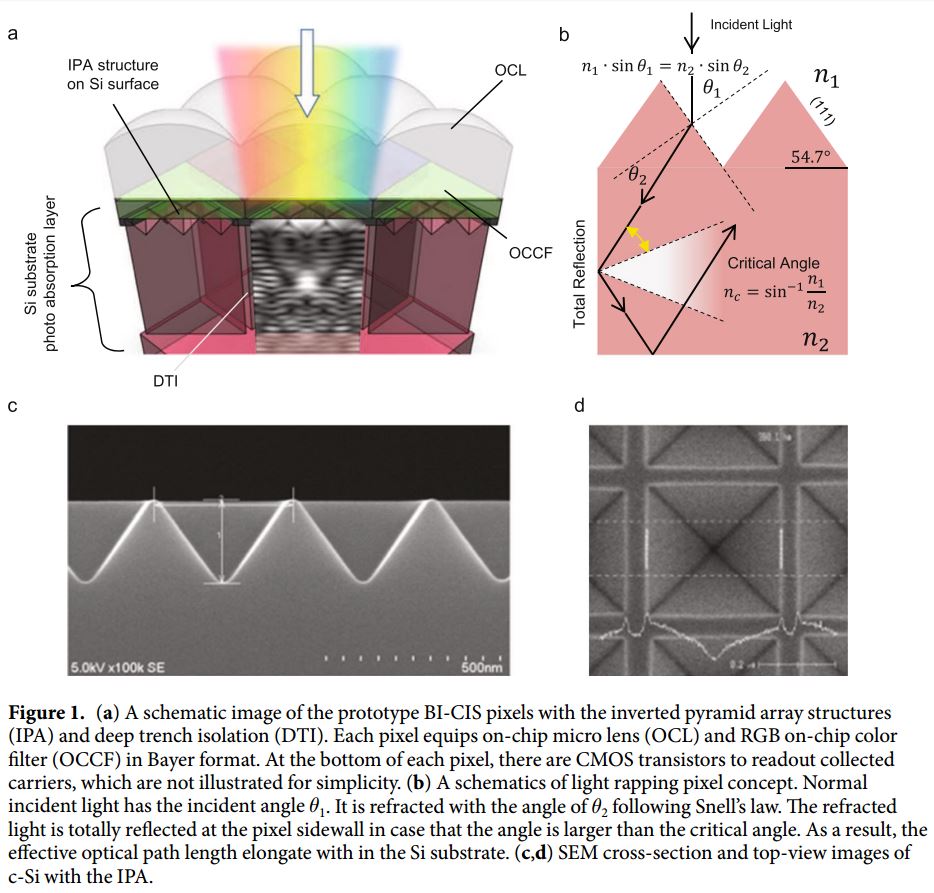
"A novel BI-CIS with IPA on c-Si surface for light trapping pixel technology is proposed and the prototyping results are demonstrated. Both spectroscopic measurements and demo images show considerable NIR sensitivity enhancement with small spatial resolution degradation. BI-CIS with 400 nm pitch IPA surface and DTI shows 80% improvement in sensitivity, which corresponds to QE of more than 30% at 850 nm for a 3 μm thick c-Si photodetector. Furthermore, it is worth noting that there is still a lot of room for improvement toward the fundamental limit of 4n^2. Additionally, it is important to control surface passivation to minimize the degradation of thermal noise and also further improve pixel isolation to reduce lateral color crosstalk as small as possible."
This technology was demonstrated in solar cell ten years ago!
ReplyDeleteDemonstrating something on a solar cell, or implementing it on a BSI-CMOS device is a slightly different story (with all respect for the solor cell guys !). So please let's be positive about new developments in the imaging technology, no matter where they come from. What you and I are doing is also based on work of others.
DeleteIt is not new in CIS community.
DeleteGoodbye Invisage. You just lost the one benefit you had over CMOS.
ReplyDeleteBullshit comment. The paper above is still using Silicon. Hence, there's a limitation to 1-1.1 um. With quantum dots you can go beyond that. Also the above paper requires fancy process technology. It's to be expected that quantum dots might have an edge on costs as well. I'm not from InVisage btw. Just annoyed by your bashing.
DeleteUnfortunately this may be very true. The gap has been narrowing already (Omni's results presented at IISW were rather striking). Invisage may still have some edge with the ability to tune the peak response more specifically, and to lay that quantum film over really small pixel pitch while retaining at least some amount of global shutter functionality (IISW again), but it is not obvious how much this is really worth to the market, weighted against the leakage penalty and presumably lack of CDS.
DeleteMy (admittedly provocative) statement was not a comment on quantum film sensors, which have a lot of potential. It was a comment on Invisage.
DeleteIt takes a lot more than a promising technology to be commercially successful. Invisage wasted huge amounts of money greedily chasing the cellphone sensor market before finally switching to focus on the NIR benefit they most-certainly offer.
Given the >$100M that's been poured in to this company, most of which has already been spent, they're going to need to demonstrate that they can make a lot of money quickly. What investor will come in now to provide working capital, knowing they'll get a highly-diluted share of the company?
High QE does not equal a good sensor in 2017. Simple things like not supporting the modes customers need can be enough to lose a slot. Sony will get these other details right. So if they can commercialize high NIR QE sensors it will diminish Invisage's potential and the chances of investors getting their money back, even if they have higher QE.
My expectation is the Invisage will turn in to a classic case study in the winner being second. Invisage will have spent all the money to prepare the technology groundwork, and then whoever comes along next gets to take it to the next level.
If an incumbent sensor supplier is interested in quantum films, putting in >$100M to pay off the existing investors makes little sense. A better strategy would be to wait till they go bankrupt and buy the IP for pennies on the dollar.
Thank you. This is a very important point to keep in mind.
DeleteRegarding questions about pushing the sensitivity past the 940nm, it is not really clear what utility this brings to applications. At 940nm we are already past the visibility, we can target the water absorption window (where there is fairly little solar energy). To go to the next water window we'd need to go past 1300nm, and I believe somewhere near 1200nm ITAR becomes involved. Yes, there is some amount of night glow showing past 1000nm as SiOnyx demonstrated, but I think that's a very specialized need, and I don't know if one can make a business servicing it.
DeleteThe conclusion of paper says “BI-CIS with 400 nm pitch IPA surface and DTI shows 80% improvement in sensitivity, which corresponds to QE of more than 30% at 850 nm for a 3 um thick c-Si photodetector.” So the actual QE at 850 nm is around 30%. I recall in IISW 2017 OmniVision showed a nearly 60% QE at 850 nm and nearly 40% QE at 940 nm. That’s about twice higher than Sony’s paper. The 40% QE at 940nm is close to what InVisage claimed. Too bad that OmniVision didn’t put it into the printed proceedings but only in the presentation. Somebody asked for the thickness of the silicon but they didn’t disclose, as far as I remembered. Did anyone know?
ReplyDeleteMore importantly, Omnivision will put it in imagers one can buy
DeleteHow's this compare to black silicone version? any one can answer?
ReplyDeleteSounds similiar to the technique sionyx is applying to their sensor
ReplyDelete