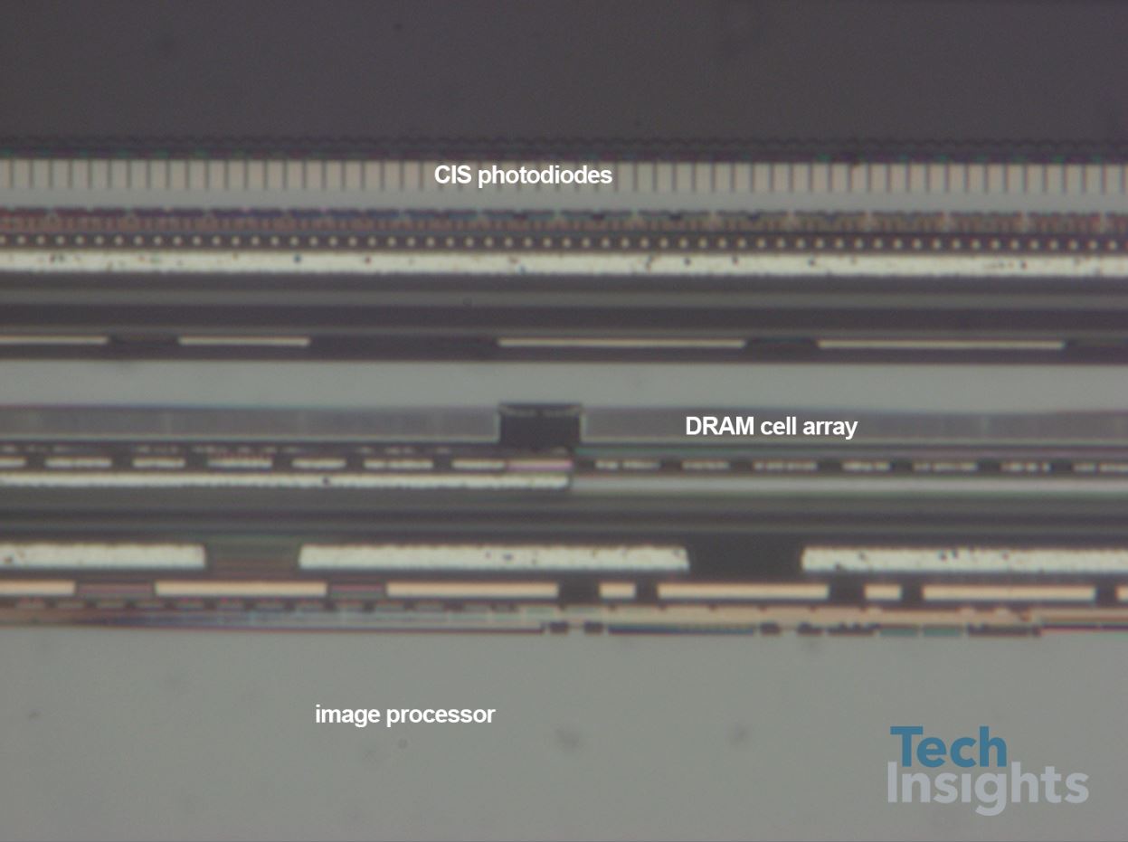
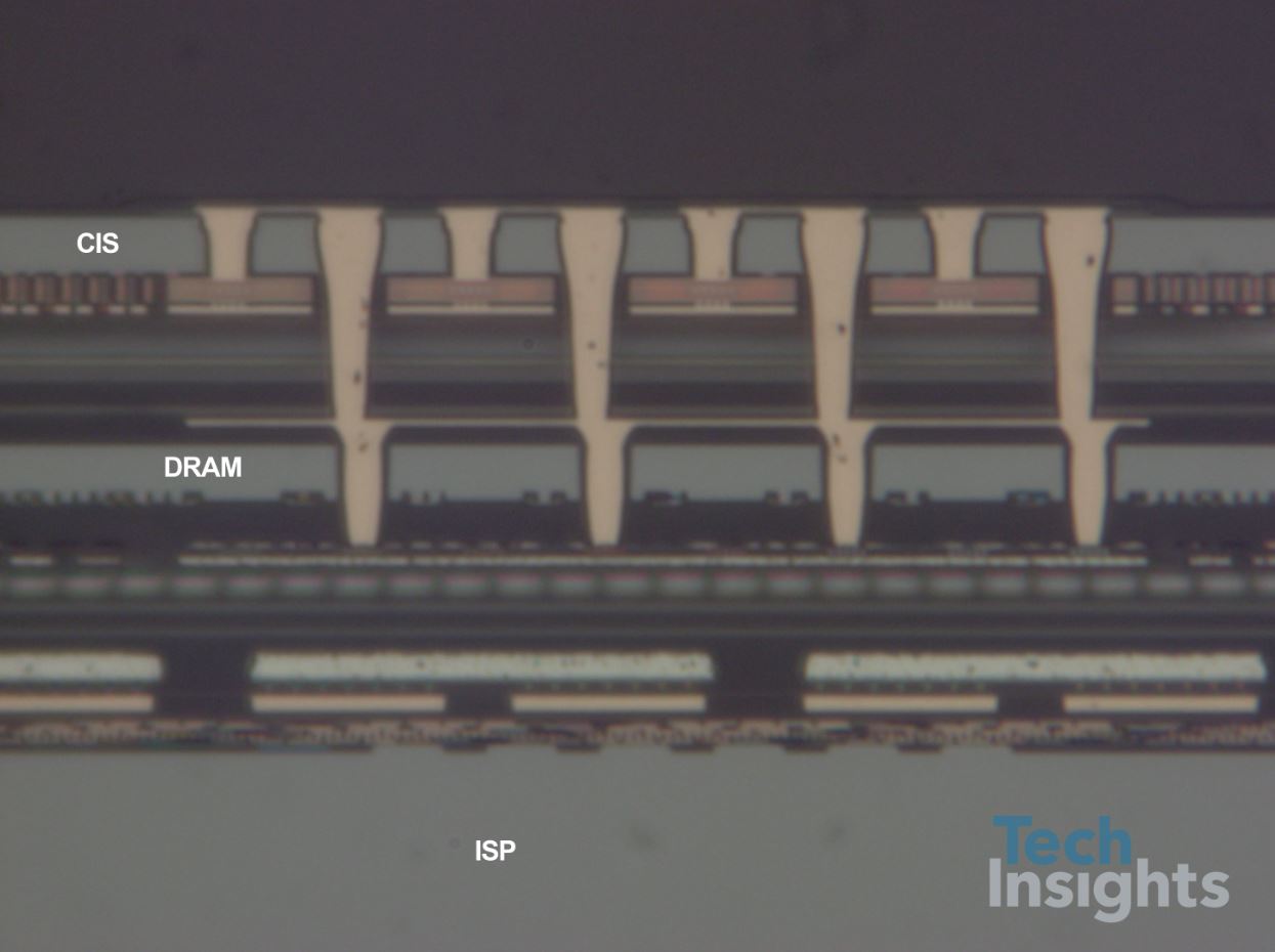
"Given that the DRAM die also has the CIS row drivers on it, then it must have been designed as a custom part, and is not one of the TSV-enabled (TSV = through-silicon via) commodity DRAMs that we have seen in recent years. Sony’s cross-section also shows that the center die has a thick back oxide and landing pad for TSVs coming down from the CIS above.
We can also see (if the scale bar is accurate), that the CIS and DRAM die substrates have been thinned down to ~2.6 µm, normal for a back-illuminated CIS (BI-CIS), but that’s the thinnest DRAM we have ever seen. Our own image (above) confirms that the CIS and DRAM silicon are of the same order in thickness, and the landing pads are also visible.
It seems likely that the CIS/ISP connection could use the DRAM landing pad layer as an interconnect, to avoid the challenge of drilling through two dies after the full stack was formed."

Thanks to RF for the info!
No comments:
Post a Comment
All comments are moderated to avoid spam and personal attacks.